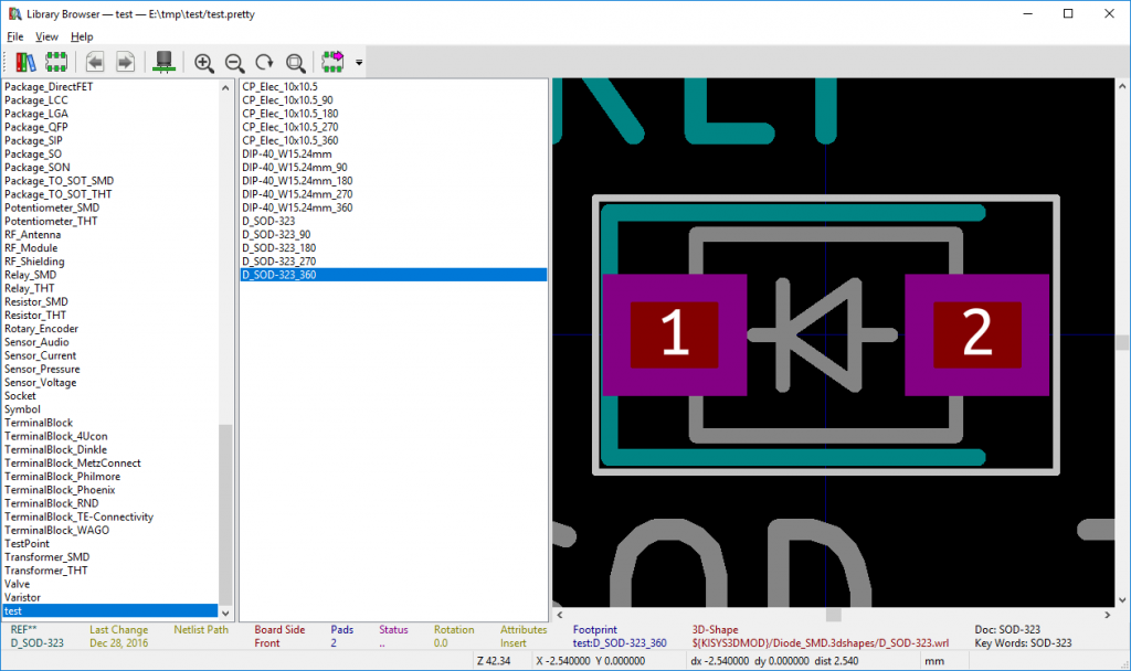
I did some reading recently on design for manufacture (in particular, https://rheingoldheavy.com/design-assembly-kicad/), and one of the things that came up was that you should have your component footprints oriented the same way as they’re loaded into the tape that gets loaded into the pick-and-place machine. Many KiCad footprints (including those that ship with KiCad) aren’t oriented this way, and even in the new KiCad 5, I don’t see an easy way to rotate an entire footprint. You can rotate a footprint inside a PCB design, but unless I’m missing something, there’s no option within the footprint editor to take all the elements within and rotate them (let alone an option to rotate an individual element, as far as I can see).
I’ve come up with this:
https://gitlab.com/salfter/kicad-footprint-rotator/
This sed script takes a KiCad footprint and rotates it 90° counterclockwise by transforming coordinates, dimensions, and rotation angles within. If you need to rotate 180°, run your footprint through the script twice. To rotate 90° clockwise, run it through three times.
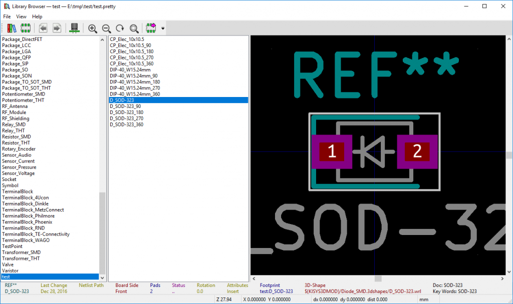
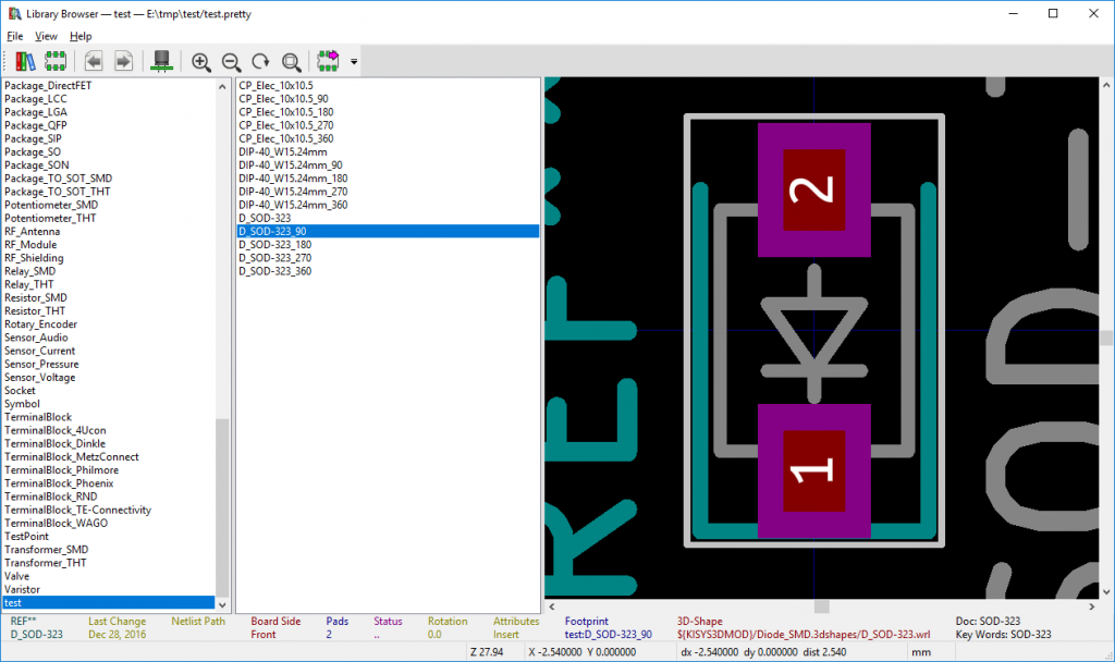
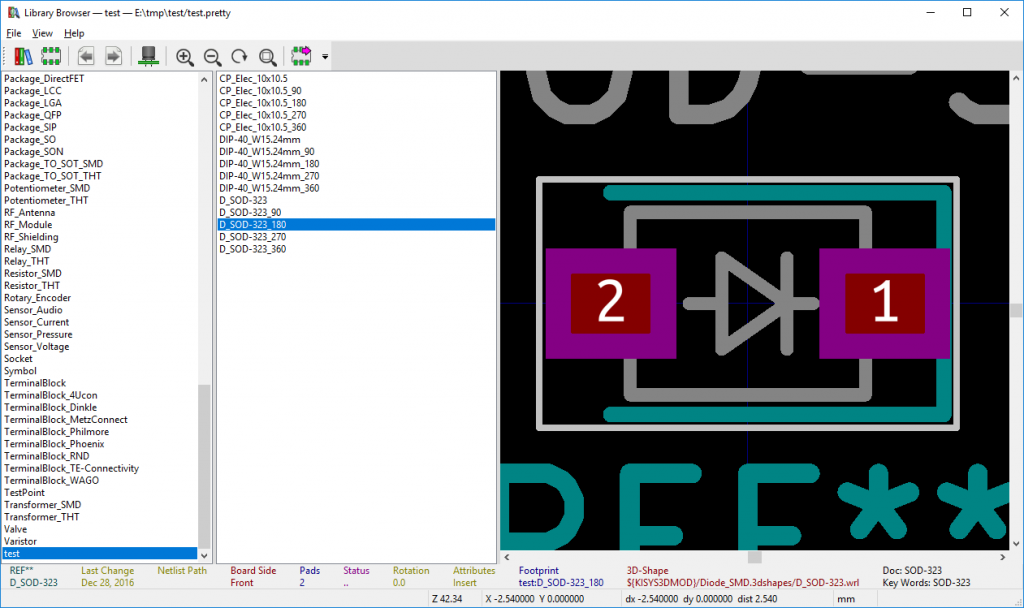
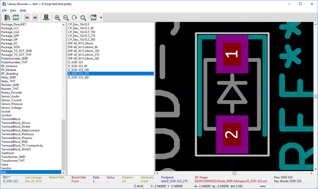
Here’s what KiCad’s SOD-323 footprint looks like as it’s rotated through 360°:
I’ve tested it on a few footprints that use different types of elements, and I think it’s working properly. That said, it’d be prudent to verify that the rotated footprint is correct before you whack it into your next project. If you run across a footprint that it screws up, I would be interested in seeing it.
